(Hong Kong)

Product Summary
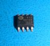
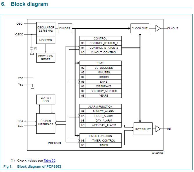
The PCF8563TF4 is a CMOS Real-Time Clock (RTC) and calendar optimized for low power consumption. A programmable clock output, interrupt output, and voltage-low detector are also provided. All addresses and data are transferred serially via a two-line bidirectional I2C-bus. Maximum bus speed of the PCF8563TF4 is 400 kbit/s. The register address is incremented automatically after each written or read data byte. The applications of the PCF8563TF4 include Mobile telephones, Portable instruments, Electronic metering and Battery powered products.
Parametrics
PCF8563TF4 absolute maximum ratings: (1)VDD, supply voltage: -0.5 to +6.5 V; (2)IDD, supply current: -50 to +50 mA; (3)VI, input voltage on pins SCL, SDA, and OSCI: -0.5 to +6.5 V; (4)VO, output voltage on pins CLKOUT and INT: -0.5 to +6.5 V; (5)II, input current at any input: -10 to +10 mA; (6)IO, output current at any output: -10 to +10 mA; (7)Ptot, total power dissipation: 300 mW; (8)Tstg, storage temperature: -65 to +150℃; (9)Tamb, ambient temperature operating device: -40 to +85℃.
Features
PCF8563TF4 features: (1)Provides year, month, day, weekday, hours, minutes, and seconds based on a 32.768 kHz quartz crystal; (2)Century flag; (3)Clock operating voltage: 1.0 V to 5.5 V at room temperature; (4)Low backup current; typical 0.25μA at VDD = 3.0 V and Tamb =25℃; (5)400 kHz two-wire I2C-bus interface (at VDD = 1.8 V to 5.5 V); (6)Programmable clock output for peripheral devices (32.768 kHz, 1.024 kHz, 32 Hz, and 1Hz); (7)Alarm and timer functions; (8)Integrated oscillator capacitor; (9)Internal Power-On Reset (POR); (10)I2C-bus slave address: read A3h and write A2h; (11)Open-drain interrupt pin.
Diagrams
 |
 PCF80 |
Other |
|
Data Sheet |
Negotiable |
|
||||
|
PCF84C00 |
Other |
|
Data Sheet |
Negotiable |
|
||||
|
PCF84C12A |
Other |
|
Data Sheet |
Negotiable |
|
||||
|
PCF84C12AP |
Other |
|
Data Sheet |
Negotiable |
|
||||
|
PCF84C21A |
Other |
|
Data Sheet |
Negotiable |
|
||||
|
PCF84C22A |
Other |
|
Data Sheet |
Negotiable |
|
||||